
- General_interview_questions_answers
- Preapring for your interview
- Analog_rfic_interview_preparation
- Question paper for analog design interview
- Another Question paper in analog integrated circuit design
- One old Question paper for Texas instruments, India, (collected)
- VLSI_design_interview_questions1
- Commonly asked interview questions
- Common entry level questions
- Common interview questions good to look at it
- VLSI_design_interview_questions2
- VLSI_design_interview_questions3
- General Electronics and communication interview question
- RF design interview question
- Typical RFIC design flow, The design flow will vary from company to company
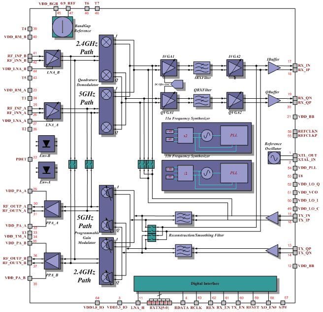
- Typical WLAN block diagram
- basic analog design reports
- Job Hunting Guide for Analog/Mixed signal Circuit Design - by Fuding Ge
- Question1: What is Slew Rate and how is it used to design an op amp?
Answer: Slew Rate (SR) is the rate at which the output voltage changes for a large scale change in voltage at the input. Thus SR is in units of volts/time. The design project specifies SR is 400nsec for a 1 volt step. This means that SR = 1V/400nsec = 2.5V/usec. Note: the slew rate is not a time, but a rate (1/time).
You will use the specification given for slew rate to determine the bias current of the differential stage, since this is the limiting charging time* (see note below). Thus you can calculate, Ibias > (SR)(Cc) and set Ibias so that it is greater than the product of the slew rate times the compensation capacitance. This equation is derived from the basic relations of
Q = C V = I t, where Q is charge and t is time.
When you calculate this value it will be rather small, and I suggest you use a current value slightly larger, maybe even 5-10 times larger, to insure you meet the SR specification.
* (note from above) The slew rate is limited either by the output of the differential amplifier or the output of the second stage, whichever is the slowest at charging the output capacitance. You can determine this from
t = (C)(V)/(I)
If we assume that we are interested in changing the charge to give a 1 volt change in output (as in your design project), then we can calculate each of these to charging times from
t = Cc/Ibias, for the differential stage
t = Cl/I6, where Cl is the load capacitor, I6 is the current in the second stage, for the second stage
(Note that both of these equations assume that the node capacitance will be dominated by Cc and Cl, which is generally a good assumption).
Since Ibias is normally much smaller than I6, the slew rate is typically limited by the differential stage and thus we write, SR = Ibias/Cc. However, you should probably check to see which of these time constants is the largest, and if you find that the second stage stage is longer, then you should adjust the currents so that SR = I6/Cl.
Wednesday, September 5, 2007
Analog and RFIC Design InterView Question
Subscribe to:
Post Comments (Atom)
No comments:
Post a Comment