
http://rfdesign.com/next_generation_wireless/broadband_technologies/synthesis-wimedia-uwb-signals-0907/
http://rfdesign.com/next_generation_wireless/broadband_technologies/709RFDF2.pdf
Friday, December 28, 2007
News - Eye catch
ADC PMC/XMC Module can be deployed in harsh environments.
Click here for product page of GE website.
Small chip, big potential
Click here for MxL5003S and here for MXL5005S.
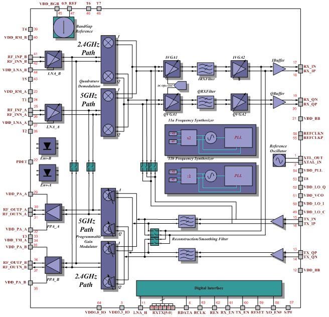
Note its archeitecture for ultra-broadband receiver.
Click here for product page of GE website.
Small chip, big potential
Click here for MxL5003S and here for MXL5005S.
Note its archeitecture for ultra-broadband receiver.
Wednesday, December 26, 2007
OFDM Baseband Receiver Design for Wireless Communications
OFDM Baseband Receiver Design for Wireless Communications
 352 pages December 2007
Description
As technologies such as mobile digital broadcasting, Wi-Fi, and WiMAX become more prevalent, increasing numbers of engineers are participating in OFDM system design. With OFDM techniques positioned to become the solution of choice for beyond 3G and 4G communications systems, the march toward single-chip solutions for small, power efficient OFDM devices is inevitable. However, up to now all OFDM books have focused on communications theory rather than hardware aspects. Composed of three sections, OFDM Baseband Receiver Design for Wireless Communications fills the gap for both signal processing and VLSI engineers with discussion of OFDM theories, algorithms, architectures and circuits.
The first section gives the reader a concise yet comprehensive look at digital communications fundamentals. Concepts behind formulas, rather than mathematical derivations, are emphasized.
The second part focuses on modern OFDM modulation and signal processing algorithms in OFDM receivers.
The third section introduces hardware design -- from design methodology to physical IC implementation -- and includes concrete examples for MC-CMDA and MIMO-OFDM WLAN.
Readers will learn how to transfer communication receiver concepts into hardware, design wireless transmitters and receivers with acceptable implementation loss, and achieve low-power designs.
Based on course materials from a highly successful graduate class in digital communication IC design, OFDM Baseband Receiver Design for Wireless Communications is aimed at senior undergraduate and graduate students of VLSI Design and Communications/Signal Processing Courses. The didactic approach also makes the topic fully accessible for experienced Engineers working on algorithms or hardware for wireless communications devices.
Tzi-Dar Chiueh receive d his Ph.D. in electrical engineering from the California Institute of Technology in 1989 and he is now a Professor of Electrical Engineering at the National Taiwan University (NTU). Since August 2004, he has also served as the Director of the Graduate Institute of Electronics Engineering at the same university. He has held visiting positions at ETH Zurich Switzerland and at the State University of New York at Stony Brook, Professor Chiueh has received the Acer longtern Award 11 times and the MXIC Golden Silicon Award in 2002 and 2005. His teaching efforts were recognized four times by the Teaching Excellence Award from the NTU. Professor Chiueh was the recipient of the Distinguished Research Achievements Award from the National Science Council, Taiwan, in 2004, and was awarded the Himax Chair Professor ship at the NTU in 2006. He is the author of more than 140 technical papers, many of which are on algorithm, architecture and integrated circuits for baseband communication systems.
Pei-Yun Tsai received her Ph.D. in electrical engineering from the National Taiwan University in 2005 and she is now an Assistant Professor of Electrical Engineering at the National central University, Taoyuan, Taiwan. Professor of Electrical Engineering at the National Central University, Taoyuan, Taiwan. Professor Tsai has received the Acer Longtern Award, MXIC Golden Silicon Award and 1s Asian Solid-State Circuit Conference Student Design Contest Outstanding Award in 2005. Her research interests include signal-processing algorithms and architectures for baseband communication systems.
352 pages December 2007Description
As technologies such as mobile digital broadcasting, Wi-Fi, and WiMAX become more prevalent, increasing numbers of engineers are participating in OFDM system design. With OFDM techniques positioned to become the solution of choice for beyond 3G and 4G communications systems, the march toward single-chip solutions for small, power efficient OFDM devices is inevitable. However, up to now all OFDM books have focused on communications theory rather than hardware aspects. Composed of three sections, OFDM Baseband Receiver Design for Wireless Communications fills the gap for both signal processing and VLSI engineers with discussion of OFDM theories, algorithms, architectures and circuits.
The first section gives the reader a concise yet comprehensive look at digital communications fundamentals. Concepts behind formulas, rather than mathematical derivations, are emphasized.
The second part focuses on modern OFDM modulation and signal processing algorithms in OFDM receivers.
The third section introduces hardware design -- from design methodology to physical IC implementation -- and includes concrete examples for MC-CMDA and MIMO-OFDM WLAN.
Readers will learn how to transfer communication receiver concepts into hardware, design wireless transmitters and receivers with acceptable implementation loss, and achieve low-power designs.
Based on course materials from a highly successful graduate class in digital communication IC design, OFDM Baseband Receiver Design for Wireless Communications is aimed at senior undergraduate and graduate students of VLSI Design and Communications/Signal Processing Courses. The didactic approach also makes the topic fully accessible for experienced Engineers working on algorithms or hardware for wireless communications devices.
Tzi-Dar Chiueh receive d his Ph.D. in electrical engineering from the California Institute of Technology in 1989 and he is now a Professor of Electrical Engineering at the National Taiwan University (NTU). Since August 2004, he has also served as the Director of the Graduate Institute of Electronics Engineering at the same university. He has held visiting positions at ETH Zurich Switzerland and at the State University of New York at Stony Brook, Professor Chiueh has received the Acer longtern Award 11 times and the MXIC Golden Silicon Award in 2002 and 2005. His teaching efforts were recognized four times by the Teaching Excellence Award from the NTU. Professor Chiueh was the recipient of the Distinguished Research Achievements Award from the National Science Council, Taiwan, in 2004, and was awarded the Himax Chair Professor ship at the NTU in 2006. He is the author of more than 140 technical papers, many of which are on algorithm, architecture and integrated circuits for baseband communication systems.
Pei-Yun Tsai received her Ph.D. in electrical engineering from the National Taiwan University in 2005 and she is now an Assistant Professor of Electrical Engineering at the National central University, Taoyuan, Taiwan. Professor of Electrical Engineering at the National Central University, Taoyuan, Taiwan. Professor Tsai has received the Acer Longtern Award, MXIC Golden Silicon Award and 1s Asian Solid-State Circuit Conference Student Design Contest Outstanding Award in 2005. Her research interests include signal-processing algorithms and architectures for baseband communication systems.
Wednesday, September 5, 2007
Analog and RFIC Design InterView Question
- General_interview_questions_answers
- Preapring for your interview
- Analog_rfic_interview_preparation
- Question paper for analog design interview
- Another Question paper in analog integrated circuit design
- One old Question paper for Texas instruments, India, (collected)
- VLSI_design_interview_questions1
- Commonly asked interview questions
- Common entry level questions
- Common interview questions good to look at it
- VLSI_design_interview_questions2
- VLSI_design_interview_questions3
- General Electronics and communication interview question
- RF design interview question
- Typical RFIC design flow, The design flow will vary from company to company
- Typical WLAN block diagram
- basic analog design reports
- Job Hunting Guide for Analog/Mixed signal Circuit Design - by Fuding Ge
- Question1: What is Slew Rate and how is it used to design an op amp?
Answer: Slew Rate (SR) is the rate at which the output voltage changes for a large scale change in voltage at the input. Thus SR is in units of volts/time. The design project specifies SR is 400nsec for a 1 volt step. This means that SR = 1V/400nsec = 2.5V/usec. Note: the slew rate is not a time, but a rate (1/time).
You will use the specification given for slew rate to determine the bias current of the differential stage, since this is the limiting charging time* (see note below). Thus you can calculate, Ibias > (SR)(Cc) and set Ibias so that it is greater than the product of the slew rate times the compensation capacitance. This equation is derived from the basic relations of
Q = C V = I t, where Q is charge and t is time.
When you calculate this value it will be rather small, and I suggest you use a current value slightly larger, maybe even 5-10 times larger, to insure you meet the SR specification.
* (note from above) The slew rate is limited either by the output of the differential amplifier or the output of the second stage, whichever is the slowest at charging the output capacitance. You can determine this from
t = (C)(V)/(I)
If we assume that we are interested in changing the charge to give a 1 volt change in output (as in your design project), then we can calculate each of these to charging times from
t = Cc/Ibias, for the differential stage
t = Cl/I6, where Cl is the load capacitor, I6 is the current in the second stage, for the second stage
(Note that both of these equations assume that the node capacitance will be dominated by Cc and Cl, which is generally a good assumption).
Since Ibias is normally much smaller than I6, the slew rate is typically limited by the differential stage and thus we write, SR = Ibias/Cc. However, you should probably check to see which of these time constants is the largest, and if you find that the second stage stage is longer, then you should adjust the currents so that SR = I6/Cl.
Free Alternatives to Matlab
Matlab・has become the de facto standard for DSP system design and simulation. However, Matlab has two problems: 1) it's expensive, and 2) it costs a lot. Fortunately, there are alternatives: Free Clones. Whatever else you can say about them, these Free Clones offer two significant advantages: 1) you don't have to pay for them, and 2) they're free.
The major Matlab clones are Scilab, Octave, and Rlab. None are true "clones", because none offer 100% compatibility with Matlab's "m-files". However, they all provide number-crunching power similar to Matlab, at a much better cost/performance ratio (since they're free!)
Essentially, Scilab, Octave, and Rlab are interpreted, matrix-based programming languages. They share with Matlab:
The use of matrices as a fundamental data type. Built-in support for complex numbers. Powerful built-in math functions and extensive function libraries. Extensibility in the form of user-defined functions.
Scilab
In some ways, Scilab may be the "best" of the Matlab clones. Scilab has many strengths, including excellent documentation (the signal processing manual is an education in itself!) and excellent support (via e-mail and its own newsgroup). Best of all, for Windows users, Scilab is supplied not only as source code, but as a Windows binary. Scilab is mostly--but not completely--compatible with Matlab. (Scilab now comes with a Matlab-to-Scilab translator, but that's still a bit immature.) For more information:
Octave
Like Scilab, Octave is another mature, high-quality Matlab clone. If you use a Unix-like operating system, Octave may be a better choice than Scilab because it reportedly offers better compatibility with Matlab. (However, for Windows users, Octave suffers the comparitive disadvantage that the binary distribution of it is quite complicated to install.) For more information:
Rlab
Rlab is the least Matlab-compatible of the three. Rlab does not try to be a Matlab clone but instead, in the words of its creator "borrows what I believe are the best features of the Matlab language and provides improved language syntax and semantics." For more information:
Others
JMathLib - A Java Clone of Octave, SciLab and Matlab
TeLa
Algae
Yorick
Euler
Python with NumPy and SciPy
The R Project for Statistical Computing (not a clone, but same matrix multiplication plus more)
The major Matlab clones are Scilab, Octave, and Rlab. None are true "clones", because none offer 100% compatibility with Matlab's "m-files". However, they all provide number-crunching power similar to Matlab, at a much better cost/performance ratio (since they're free!)
Essentially, Scilab, Octave, and Rlab are interpreted, matrix-based programming languages. They share with Matlab:
The use of matrices as a fundamental data type. Built-in support for complex numbers. Powerful built-in math functions and extensive function libraries. Extensibility in the form of user-defined functions.
Scilab
In some ways, Scilab may be the "best" of the Matlab clones. Scilab has many strengths, including excellent documentation (the signal processing manual is an education in itself!) and excellent support (via e-mail and its own newsgroup). Best of all, for Windows users, Scilab is supplied not only as source code, but as a Windows binary. Scilab is mostly--but not completely--compatible with Matlab. (Scilab now comes with a Matlab-to-Scilab translator, but that's still a bit immature.) For more information:
- Scilab Home Page
- Scilab Documentation and Support Page
- Scilab Online Documentation
- Scilab
Signal Processing Toolbox Functions - Scilab Download Page
Octave
Like Scilab, Octave is another mature, high-quality Matlab clone. If you use a Unix-like operating system, Octave may be a better choice than Scilab because it reportedly offers better compatibility with Matlab. (However, for Windows users, Octave suffers the comparitive disadvantage that the binary distribution of it is quite complicated to install.) For more information:
Rlab
Rlab is the least Matlab-compatible of the three. Rlab does not try to be a Matlab clone but instead, in the words of its creator "borrows what I believe are the best features of the Matlab language and provides improved language syntax and semantics." For more information:
Others
JMathLib - A Java Clone of Octave, SciLab and Matlab
TeLa
Algae
Yorick
Euler
Python with NumPy and SciPy
The R Project for Statistical Computing (not a clone, but same matrix multiplication plus more)
Sunday, August 19, 2007
Cadence Customer Support Solution 11175734
PHASE NOISE IS NOT CONSISTENT FOR PNOISE SOURCES AND JITTER IN ADE
Problem statement:
You are running a PSS/PNOISE analysis on an autonomous circuit in Analog Design Environment. You first set a pnoise=sources and then a pnoise= jitter in the analysis form. After running both simulations and plotting the results from the Direct Plot form, you notice a 3db difference between the phase noise from Pnoise->sources and Pnoise-> Jitter . Why?
Solution:
When you run pnoise=sources, spectreRF just calculates the noise as the time-average power spectral density and therefore does not provide correlations in the noise and so the cyclostationary nature of the noise. The output noise is the voltage noise, just as it would be measured by an oscilloscope. The pnoise=source analysis does not separate Voltage noise into AM and PM components. The phase noise is therefore being calculated as the output noise scaled back by the power in the carrier.Indeed, for autonomous case and close to the carrier, entire noise is phase noise, so we can substitute S_v for S_phi in dBc units. This assumption is not valid away from the carrier.
When running pnoise-> Jitter for autonomous circuit, spectreRF invokes in the background pnoise modulated analysis that captures the full cyclostationary nature of the noise. Pnoise modulated analysis uses the spectrum along with information about the correlations in the noise between sidebands. This analysis figures out correlation between upper and lower sideband. Based on relation between USB and LSB, spectreRF assesses the level of AM and PM noise.
The difference observed hence occurred because Pnoise-> Jitter does compute PM/AM components and uses correct definition of the phase noise whereas Pnoise->Sources is using the fact that in special case (for autonomous circuit close to the carrier, see above) the whole noise is due to the PM component. Assuming your circuit is fully matched, you should therefore see a 3 dB difference between phase noise (3dB is the result of is the scale of two was due to usage of one sided PSD in PNOISE).
Source:http://sourcelink.cadence.com/docs/db/kdb/2005/Apr/11175734.html
Wednesday, August 15, 2007
Tuesday, August 14, 2007

Subscribe to:
Comments (Atom)